
Silicon sits quietly at the centre of modern life. It powers the phone in your hand, solar panels on rooftops, engine sensors in cars, and medical devices in hospitals. Without silicon, the digital economy stops.
Despite that reach, most explanations of silicon stop at one of two extremes: a chemistry-textbook definition of an element or a deep dive into chip fabrication that assumes you already know the basics. This guide bridges both worlds.
We will follow silicon from beach sand to finished semiconductor wafers, explain why the same element behaves as an insulator, conductor, and semiconductor depending on how it is prepared, and clarify the difference between silicon and silicone once and for all.
Why Does Silicon Matter From Earth’s Crust to Modern Industry?
Silicon is the second most abundant element in Earth’s crust by mass, making up roughly 28% of the planet’s outer layer. Only oxygen is more common. This abundance is one reason silicon dominates industry: it is widely available, distributed across nearly every continent, and chemically stable enough to ship and store without specialised handling.
Silicon supports multiple global industries
According to Grand View Research, the global silicon metal market was valued at approximately $14.5 billion in 2024, driven by demand from aluminium alloys, chemicals, and solar photovoltaics. The semiconductor industry, which depends on ultra-purified silicon, is also one of the world’s most valuable manufacturing sectors.
Silicon touches three distinct industries that rarely intersect:
- Construction and chemicals consume ferrosilicon and silica in cement, glass, and silicone polymers.
- Aluminium and steel use silicon as an alloying agent to improve strength and castability.
- Electronics and solar consume high-purity silicon for wafers and photovoltaic cells.
| Industry | Silicon material used | Common applications |
| Electronics | Electronic-grade silicon | Chips, sensors, processors, memory |
| Solar energy | Solar-grade silicon | Photovoltaic cells and solar modules |
| Automotive | Aluminium-silicon alloys | Engine blocks, wheels, transmission housings |
| Construction | Silica and silicone materials | Glass, sealants, coatings, insulation |
| Medical | Silicone polymers | Tubing, seals, moulded components |
| Chemicals | Silanes and fumed silica | Adhesives, paints, cosmetics, toothpaste |
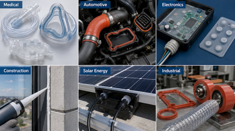
A solar farm needs substantial volumes of silicon-derived materials to produce photovoltaic panels, while semiconductor manufacturing depends on extremely pure silicon for wafers and microchips.
Why Can Silicon Behave So Differently?
The key difference is purity. Impurities in silicon are not simply contaminants; they can actively change electrical behaviour. A piece of silicon containing iron behaves very differently from highly purified silicon intentionally doped with trace amounts of boron or phosphorus.
The semiconductor industry has spent decades learning to remove, control, and deliberately reintroduce specific atoms into silicon’s crystal lattice. That control is the foundation of every modern microchip.
What Are Silicon’s Main Physical and Chemical Properties?
Silicon sits in Group 14 of the periodic table, directly below carbon and above germanium, tin, and lead. It has the symbol Si, atomic number 14, and an atomic mass of 28.0855.
Its four valence electrons are especially important for engineering applications. They allow silicon to form four covalent bonds, creating the tetrahedral crystal structure that shapes its physical and electronic behaviour.
Silicon is a metalloid
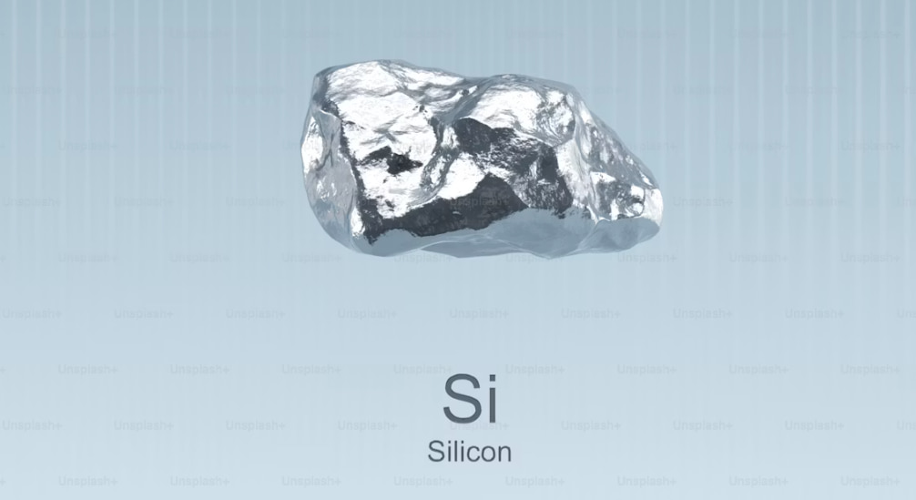
Silicon is classified as a metalloid, meaning it shares properties with both metals and non-metals. Pure crystalline silicon has a metallic grey appearance, but it is brittle rather than ductile. Its electrical conductivity sits between that of a conductor and an insulator.
Silicon’s conductivity also increases with temperature and is highly sensitive to small amounts of impurities. This controlled introduction of impurities is known as doping.
| Property | Typical value | Engineering significance |
| Atomic number | 14 | Defines valence electron count |
| Atomic mass | 28.0855 u | Basis for isotope separation |
| Density | 2.329 g/cm³ | Lightweight for handling and shipping |
| Melting point | 1,414 °C | Determines furnace design for refining |
| Boiling point | 3,265 °C | Sets limits for high-temperature processes |
| Crystal structure | Diamond cubic | Defines cleavage, slip, and doping behaviour |
| Bandgap at 300 K | 1.12 eV | Supports microelectronics applications |
| Thermal conductivity | 148 W/m·K | Helps wafers manage heat |
| Mohs hardness | 6.5 | Harder than glass but softer than quartz |
| Common isotopes | Si-28, Si-29, Si-30 | Si-28 enrichment supports quantum research |
The 1.12 eV bandgap helps explain why silicon dominates microelectronics. It is large enough for pure silicon to act as an insulator at room temperature, yet small enough for modest heating or doping to produce useful electrical conduction.
Materials such as gallium arsenide can offer higher performance in specific applications, but silicon remains more economical, widely available, and easier to grow into large crystals. Its native oxide, silicon dioxide or SiO₂, is another major advantage for semiconductor manufacturing.
Where Does Silicon Come From Naturally?
Silicon almost never occurs in pure form in nature. It is usually bonded with oxygen as silica, SiO₂, or combined with oxygen and metals as silicate minerals. Roughly 90% of Earth’s crust consists of silicate minerals, and quartz is one of the most familiar pure forms of silica.
Quartz is silicon’s common industrial starting point
Quartz forms from silica-rich solutions over geological timescales, often in granitic and metamorphic rocks. Industrial quartz is mined from high-purity deposits in countries including the United States, Norway, China, and Russia.
Quartz has a Mohs hardness of 7, a melting point of approximately 1,650 °C, and piezoelectric properties that make it useful in oscillators, filters, and precision timing devices. However, most quartz is used in glass, foundry sand, ceramics, and silicon metal production rather than electronics.
Not all beach sand is suitable for silicon production
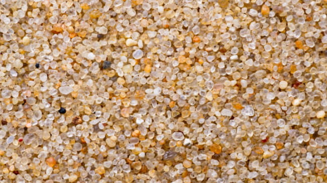
Industrial silicon feedstock requires high-purity quartzite or quartz sand containing at least 99.5% SiO₂, with very low levels of iron, aluminium, and boron.
Boron is particularly problematic because it acts as a p-type dopant in the final silicon and cannot be removed economically during later refining. Converting natural quartz into high-purity silicon is therefore a step-by-step purification process that balances purity, energy use, and cost.
What Is the Difference Between Silicon and Silicone?
Silicon and silicone are commonly confused because their names are similar, but they are entirely different materials with different properties, uses, and supply chains.
Silicon is an element, while silicone is a polymer
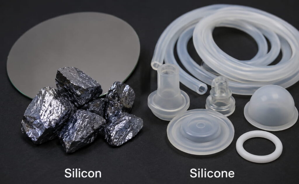
Silicon is a chemical element with atomic number 14. Silicone is a synthetic polymer built around a backbone of alternating silicon and oxygen atoms, usually with methyl groups attached to the silicon atoms.
The most common silicone, polydimethylsiloxane or PDMS, does not resemble elemental silicon in appearance or behaviour.
| Property | Silicon | Silicone |
| Chemical nature | Element, Si | Polymer, [–Si(CH₃)₂–O–]ₙ |
| Form | Grey crystalline solid | Flexible rubber, oil, or resin |
| Electrical behaviour | Semiconductor | Insulator |
| Thermal stability | High, melts at 1,414 °C | Typically stable from around -50 to 250 °C |
| Typical uses | Chips, solar cells, alloys | Sealants, cookware, medical devices |
| Density | 2.33 g/cm³ | Usually 0.97 to 1.5 g/cm³ |
| Appearance | Metallic grey and brittle | Translucent and flexible |
| Toxicity | Generally low, though dust can be hazardous | Generally low when correctly specified |
Correct terminology matters for B2B buyers
The distinction has practical commercial consequences. A procurement officer searching for a silicone gasket supplier needs a flexible elastomer, while a silicon wafer supplier provides a brittle semiconductor material.
Specifying the correct material in an RFQ, certificate of analysis, or regulatory filing is not a minor detail. It can determine whether a buyer receives a flexible elastomer or a semiconductor wafer.
For applications involving seals, medical parts, coatings, or flexible moulded components, it is useful to understand how silicone rubber performs across major industries, particularly where heat, electrical insulation, long service life, or compliance requirements are involved.
What Are the Main Silicon Purity Grades?
Purity is one of the most important specifications in silicon sourcing. It is commonly expressed through the number of “nines”, with each additional nine representing a major reduction in impurity concentration and a substantial rise in value.
Silicon grades range from metallurgical to electronic grade
| Grade | Typical purity | Typical impurity level | Primary use |
| Metallurgical-grade silicon | 98 to 99% | 10,000+ ppm | Aluminium alloys, silicones, steel |
| Chemical-grade silicon | 99.5 to 99.9% | 100 to 5,000 ppm | Silicones, fumed silica, some solar applications |
| Solar-grade silicon | 99.9999% or 6N | Less than 1 ppm | Solar cells and lower-end electronics |
| Electronic-grade silicon | 99.9999999% or 9N | Less than 0.01 ppb | Semiconductor wafers and integrated circuits |
| Prime wafers | Up to 11N purity | Less than 0.001 ppb | Advanced logic and memory chips |
Silicon grade selection depends on the final application
| Requirement | Suitable grade | Why it is suitable |
| Steelmaking and aluminium alloys | Metallurgical-grade silicon | Delivers alloying benefits without unnecessary purification cost |
| Silicone polymer production | Chemical-grade silicon | Supports more controlled downstream chemical processing |
| Photovoltaic cells | Solar-grade silicon | Provides sufficient purity for energy conversion |
| Semiconductor chips and sensors | Electronic-grade silicon | Enables tightly controlled electrical performance |
| Advanced logic and memory | Prime wafer material | Meets strict purity and surface-finish requirements |
The transition from metallurgical-grade to electronic-grade silicon is one of the most demanding purification challenges in industrial chemistry. The Siemens process remains a dominant route, using the decomposition of trichlorosilane on heated silicon rods to create high-purity polysilicon.
Higher purity creates higher-value silicon
Price scales nonlinearly with purity. As of 2024, metallurgical silicon traded around $2-3 per kilogram, chemical grade around $3-5, solar grade in the $6-10 range, and electronic-grade polysilicon between $20-40 per kilogram for spot orders. Finished prime wafers, polished and ready for fabrication, can exceed $200 per wafer for the largest diameters.
How Does Silicon Go From Sand to a Semiconductor?
The route from quartz to a finished chip involves multiple stages, each with its own equipment, energy requirements, and quality controls.
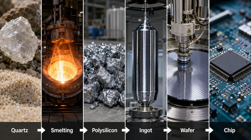
The silicon supply chain at a glance
| Stage | Main process | Output | Why it matters |
| 1 | Quartz mining and beneficiation | High-purity quartz feedstock | Removes unwanted minerals before refining |
| 2 | Carbothermic reduction | Metallurgical-grade silicon | Converts silica into elemental silicon |
| 3 | Chemical purification | Trichlorosilane | Separates metallic and dopant impurities |
| 4 | Siemens process | Electronic-grade polysilicon | Produces ultra-pure silicon feedstock |
| 5 | Crystal growth | Monocrystalline silicon ingot | Creates the structure required for wafers |
| 6 | Wafer slicing and polishing | Finished silicon wafers | Produces smooth surfaces for chip fabrication |
| 7 | Device fabrication | Integrated circuits | Turns wafers into functioning electronic devices |
Stage 1: Quartz mining and beneficiation
High-purity quartz is mined, crushed, washed, and sorted. Magnetic separation removes iron-bearing minerals, froth flotation separates feldspar and mica, and acid leaching removes remaining surface contaminants.
The output is quartz feedstock with at least 99.5% SiO₂ and low boron content.
Stage 2: Metallurgical-grade silicon production
Quartz is reduced with carbon, such as coke, coal, or wood chips, in a submerged-arc electric furnace at approximately 1,500 to 2,000 °C. This carbothermic reduction process produces metallurgical-grade silicon with 98 to 99% purity.
This is the most important chemical step in silicon production. The furnaces are among the largest in industry and can consume 12 to 14 MWh of electricity per tonne of silicon.
Stage 3: Chemical purification into trichlorosilane
Metallurgical-grade silicon reacts with anhydrous hydrogen chloride at around 300 °C to create trichlorosilane, HSiCl₃. This material is purified through fractional distillation.
Distillation removes boron, phosphorus, and many metallic impurities because their chlorides have different boiling points.
Stage 4: The Siemens process produces electronic-grade polysilicon
Purified trichlorosilane is decomposed on heated silicon rods inside bell-jar reactors. Silicon deposits atom by atom onto the rods, gradually forming dense polycrystalline silicon.
The output is electronic-grade polysilicon, generally at 9N purity or higher.
Stage 5: Monocrystal growth creates silicon ingots
Polysilicon is melted in a quartz crucible. A seed crystal is dipped into the melt, then slowly pulled upward and rotated. As the molten material solidifies, it forms a single-crystal silicon ingot.
The Czochralski process is widely used for 200 mm and 300 mm wafers. Float-zone growth is used for higher-purity applications because it moves impurities along the silicon rod rather than trapping them in the crystal.
Stage 6: Wafers are sliced, etched, and polished
The silicon ingot is ground to a precise diameter, notched for orientation, and sliced into wafers using a wire saw or diamond saw. A 300 mm wafer is typically around 775 µm thick before final processing.
The wafers are then lapped, etched, polished, and cleaned to achieve an extremely smooth surface with less than 0.5 nm roughness.
Stage 7: Device fabrication turns wafers into chips
Each polished wafer enters a semiconductor fabrication facility, where it undergoes lithography, etching, deposition, implantation, and other processes to form integrated circuits.
That work takes place in cleanrooms where even a single dust particle can damage a chip.
How Does Silicon Become a Semiconductor?
Pure silicon is a poor conductor at room temperature because its four valence electrons are bound in covalent bonds. Doping and bandgap control turn it into the semiconductor material used in modern electronics.
N-type and p-type silicon are created through doping
Doping introduces selected impurity atoms into the silicon crystal lattice.
Adding pentavalent elements such as phosphorus, arsenic, or antimony creates an extra electron that can move through the material. This produces n-type silicon.
Adding trivalent elements such as boron, gallium, or indium creates a missing electron, known as a hole, that behaves as a positive charge carrier. This produces p-type silicon.
Although dopant concentrations are extremely low compared with the number of silicon atoms in the crystal, the electrical effect is substantial.
P-N junctions make modern electronics possible
Placing n-type and p-type silicon together forms a p-n junction. This acts as a one-way control point for electrical current and is the basis of diodes, transistors, solar cells, and many other electronic devices.
By arranging multiple junctions in controlled geometries, engineers create transistors that switch billions of times per second.
Why Is Silicon Used in Solar Panels?
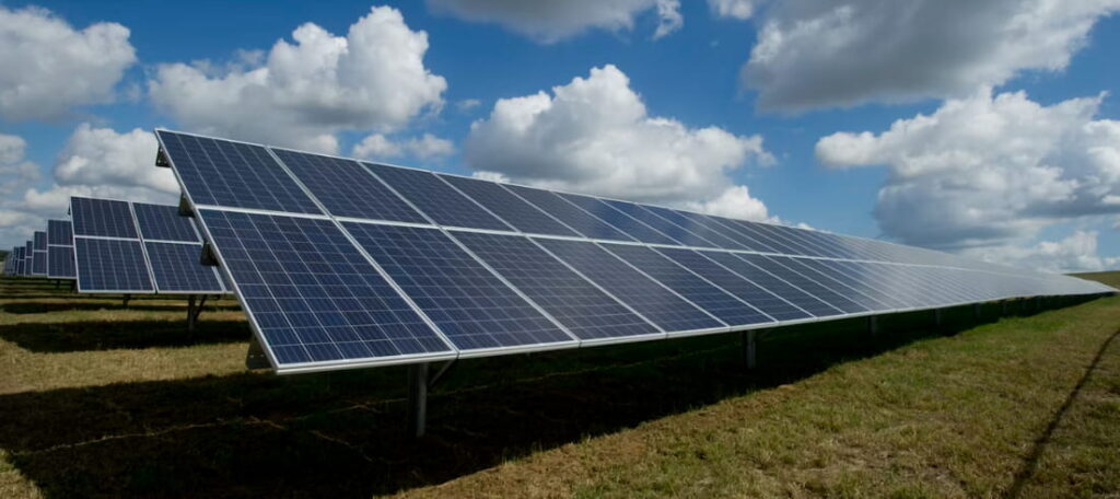
Solar cells are the second major use for high-purity silicon after microelectronics. Semiconductor fabs often require 9N to 11N purity, while solar cells generally work effectively with silicon at 6N to 7N purity.
Monocrystalline cells provide higher efficiency
Monocrystalline solar cells are cut from single-crystal ingots, like those used in microelectronics, and can achieve efficiencies of 22 to 26%. Multicrystalline cells are cast in blocks, contain multiple grain boundaries, and generally achieve efficiencies of 18 to 22%.
The solar market continues to move towards monocrystalline cells and larger wafer formats, including 182 mm and 210 mm wafers.
Silicon remains the dominant photovoltaic material
Silicon’s 1.12 eV bandgap works well with the solar spectrum. It is abundant, non-toxic, stable, and supported by a mature global supply chain.
Thin-film materials such as cadmium telluride and copper indium gallium selenide can perform well in specific applications, but silicon remains the standard choice for utility-scale solar because of its established manufacturing base and long-term reliability.
While silicon forms the photovoltaic cell itself, silicone materials are often used around the system for sealing, bonding, and environmental protection. For a closer look at these applications, see silicone in renewable energy systems.
Where Is Silicon Used Beyond Electronics?
Most silicon does not become a semiconductor wafer or solar cell. Metallurgical-grade silicon is also essential in aluminium alloys, chemicals, sealants, and advanced ceramics.
Aluminium-silicon alloys improve casting performance
Adding 5 to 20% silicon to aluminium produces alloys that are lighter, more castable, and more wear-resistant than pure aluminium.
Aluminium-silicon alloys are widely used for engine blocks, cylinder heads, transmission housings, and automotive wheels.
Silicones, silanes, and fumed silica support everyday products

Silicon reacts with methyl chloride to create methylchlorosilanes, which are used to manufacture silicone polymers. PDMS is widely used in sealants, cookware, medical devices, lubricants, and cosmetics.
Fumed silica, produced by burning silicon tetrachloride in a flame, is a thickening agent in products such as toothpaste, paint, and adhesives.
For medical uses, silicone selection should account for formulation, biocompatibility, curing method, and compliance needs. Read our guide on HCR silicone for medical applications for a more detailed overview.
Silicon carbide and silicon nitride are advanced ceramics
Silicon carbide, SiC, and silicon nitride, Si₃N₄, are advanced ceramics used in abrasive applications, refractory linings, and high-temperature structural components.
Silicon carbide is increasingly important in electric vehicle power electronics because it can operate at higher voltages and frequencies than conventional silicon devices.
What Does the Future of Silicon Look Like?
Three forces are reshaping silicon demand: artificial intelligence, the energy transition, and semiconductor supply-chain localisation.
AI depends on accelerators and high-bandwidth memory built using advanced semiconductor processes. Solar energy depends on silicon-based photovoltaic cells, while electric vehicle power electronics increasingly use silicon carbide. Governments across the United States, Europe, Japan, and other regions are also investing in domestic semiconductor production to reduce supply-chain concentration.
Silicon sourcing requires closer planning
For procurement and engineering teams, silicon is no longer a material that can always be treated as a simple commodity. Availability, purity grade, lead time, processing requirements, and supply-chain risk can all affect sourcing decisions.
For energy-sector applications, the surrounding silicone materials also need to withstand heat, UV exposure, electrical stress, weathering, and long service periods.Our guide to HCR silicone for energy-sector applications explains these performance requirements in more detail.
Conclusion
Silicon remains one of the world’s most important industrial materials because it supports everything from semiconductors and solar panels to aluminium alloys, glass, chemicals, and advanced ceramics. Understanding its purity grades, natural sources, processing route, and electrical behaviour helps buyers and engineers select the right material for the correct application.
At Flexion, we help customers turn silicone material requirements into dependable parts for medical, automotive, consumer, industrial, and energy applications. As a manufacturer of various types of Silicone in Thailand, we support custom formulations, moulding, extrusion, coating, and production planning for projects that require reliable flexibility, temperature resistance, electrical insulation, and long-term performance.
Common Questions About Silicon
Is silicon a metal or non-metal?
Silicon is a metalloid, meaning it shares properties with both. It has a metallic grey appearance and can conduct electricity, but it is brittle and its conductivity depends heavily on temperature and impurities.
What is silicon used for in everyday life?
Silicon is used in integrated circuits, smartphones, computers, vehicles, solar panels, glass, ceramics, aluminium alloys, sealants, cookware, and quartz watches.
Is silicon toxic to humans?
Elemental silicon is generally considered low risk. However, respirable crystalline silica dust can cause silicosis, a serious lung disease. Quartz mining, cutting, and sandblasting operations require strict dust-control measures. Silicone polymers are also widely used in medical applications when correctly specified.
How is silicon different from silica?
Silicon is the element Si. Silica is silicon dioxide, SiO₂, formed when silicon bonds with oxygen. Silica occurs naturally as quartz, sand, and many other mineral forms.
Where is most silicon produced?
China is a major producer of metallurgical silicon, alongside countries such as Brazil, the United States, Norway, and Russia. Electronic-grade polysilicon production is more concentrated among specialist producers in Germany, the United States, South Korea, Japan, and China.
Why is silicon used in computer chips instead of germanium?
Silicon forms a stable native oxide, SiO₂, that is electrically insulating and easy to grow. This oxide is fundamental to MOSFET technology and modern integrated circuit manufacturing. Germanium offers higher electron mobility but lacks an equally useful native oxide.
Can silicon conduct electricity?
Pure silicon is a poor conductor at room temperature. However, doped silicon can conduct electricity very effectively. N-type silicon uses dopants such as phosphorus, while p-type silicon uses dopants such as boron.
What is the difference between polysilicon and monocrystalline silicon?
Polysilicon contains many small crystal grains and is commonly used as feedstock for additional processing. Monocrystalline silicon is one continuous crystal with no grain boundaries, making it suitable for semiconductor wafers and high-efficiency solar cells.
How much silicon is in a smartphone chip?
A typical 300 mm wafer contains roughly 8 to 10 grams of silicon and can produce hundreds of chips. The amount of raw silicon in an individual smartphone chip is very small, but the processing value added to that material is substantial.
Will silicon be replaced by another chip material?
Silicon will remain dominant in most logic and memory applications because of its native oxide, mature supply chain, and enormous existing manufacturing infrastructure. Materials such as silicon carbide and gallium nitride are increasingly important in power electronics and radio-frequency applications, while isotopically pure silicon is being explored for quantum computing.